At the ILC, roughly 16,000 superconducting RF cavities made of pure niobium will accelerate electrons and positrons to the high energy of 500 GeV. Each one-metre-long cavity consists of nine cells, polished to provide micrometre-level surface smoothness and absolutely no impurities. The inside of the cavities need to literally sparkle since any surface blemishes or dust could cause them to lose their superconductivity, making them unable to sustain the electric field needed to accelerate particles. ILC scientists around the world are devoted to trying to get a higher yield rate for producing good-quality cavities by improving surface treatment methods and inspection procedures. A group of scientists from Kyoto University and KEK jointly developed the novel inspection system to take a close look at the interior surface of the cavities, and produced remarkable results.
 High-resolution surface inspection camera for superconducting cavities with Yoshihisa Iwashita (left) and Yujiro Tajima (right) from Kyoto university. |
To inspect the cavity's interior surface, scientists conduct the tests like passband mode or thermometry measurements to identify the location of the spots which limit the cavity's performance. Scientists have been using a device very similar to a gastric camera to look into the cavity, but could not see any spot at the location identified by tests. The project of developing the technology for a cavity camera started from a small chat at one of the conferences. “Dr. Hitoshi Hayano and I talked about collaborative projects between KEK and Kyoto University, in which the university would play a proactive role. We discussed about possible tasks and decided to pursue R&D on a high-resolution camera for cavity inspection,” Yoshihisa Iwashita from Kyoto University said. He talked to Yujiro Tajima, who was an undergraduate student at the time, to tackle this task.
The idea was rather simple: inserting a compact high-resolution camera directly into the cavity. But to develop that device was not so simple. Most of the components for this innovative camera are ready-made products, but putting them together to make them work as they wanted was a challenge. Tajima recalls, “Even if one small component was not properly assembled, the overall system did not work. That made me think that the big machine like ILC is the same; the vast number of technologies accurately assembled for ILC to work as intended.”
 ... and extracted from a cavity. |
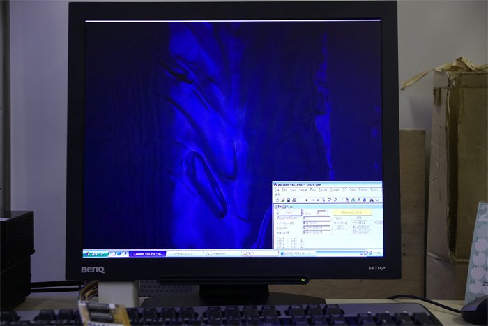
 Digital image taken by the high-resolution surface inspection camera. |
This high-resolution camera is placed into the 50-millimetre cylinder, and no parts will pop out from the system at the shooting, getting rid of the threat of damaging the carefully treated cavity interior. Lighting inside the cavity posed a challenge since its interior is just like a mirror. To solve the problem, Tajima used fourteen Electro-Luminescence (EL) strip sheets, wrapping them around the cylinder, enabling him to measure wall gradients of the cavity's interior surface. “EL has started to garner attention as a technology for low-profile TV, but the technology itself has been around for 20 years. What lead this R&D to success are not the technologies used in this camera, but Hitoshi's foresight and Yujiro's passion,” Iwashita said.
Iwashita's team found less than 100 micrometre level spots that correlate with thermometry measurements conducted at Fermilab and JLab. This camera could identify the location, size and shape of the spots, making it possible for scientists to judge the cause. It will lead to improving the cavity treatment method, thus improving the yield. This camera would make an important milestone for future mass production of high-gradient cavities for ILC.
“I would like to work at the ILC, the project with the big dream,” Tajima said. Looking inside the cavity will help make his dream come true.
-- Rika Takahashi
