Director's Corner
26 March 2009
 Marc Ross |
Renewing links with superconducting cavity manufacturers
Today's issue features a Director's Corner from Marc Ross, Project Manager for the Global Design Effort.
The most important performance parameter for a linear accelerator is its cost per electronvolt of accelerated beam, or cost per watt of delivered beam power. In the early 1990s, a core group of experts from labs in each today’s ILC regions Americas, Asia and Europe, concluded that the so-called 'cold technology', based on superconducting radiofrequency (rf), could effectively compete with traditional 'warm technology' for the next energy frontier machine, the linear collider. They then set about to prove the cold technology was a cost-effective alternative through the TESLA collaboration and through partnerships with cavity manufacturing companies. This guest Director's Corner is about our effort to open new relationships and partnerships with these companies, worldwide.
In a very broad sense, the biggest challenge to achieving very high performance in a superconducting rf cavity is to keep it cold. For ILC cavities, the sheet metal niobium must be pure and well formed into the intended elliptical cell shape, free of defects such as cracks or pits. For the one-metre-long nine-cell cavities we will use, this task is done by and large by cavity fabrication companies. Following the fabrication, the inner surface must be cleaned of dust, fingerprints and other contaminants before testing. Because of tight coupling between the cleaning, assembly and testing processes, this task is typically done at labs, using their extensive infrastructure.
Throughout the 1990s, the fabrication process was studied and perfected using experience gained at big projects based at CERN, DESY, CEBAF, Cornell and KEK. At the time of the formation of the ILC Global Design Effort in 2005, it was reported that the most important challenge to high-gradient performance was field emission. Field emission is typically caused by contaminants like the ones mentioned above. Experts from the newly-named TESLA Technology Collaboration suggested the adaptation of processes not unlike those used in a household dishwasher to clean the inner surface of the cavity, and in the last few years we have seen (and reported in this column) their recommendations succeed. In 2008 only 15 percent of the cavity tests performed at JLab were limited by field emission.
It is now time, once again, to turn our attention to performance limitations caused by the fabrication process. With this in mind, the ILC GDE Project Managers sought the possibility of visiting each of the world's major cavity fabrication companies. Our aim was to report our recent global progress to them, to describe the Technical Design Phase R&D Plan and solicit their reports and comments and ask them about the issues surrounding their activities. We also wished to express our intention to establish communication channels to promote the development of a confident, reliable relationship. Our visits were facilitated in cooperative effort with the GDE regional and institutional leaders.
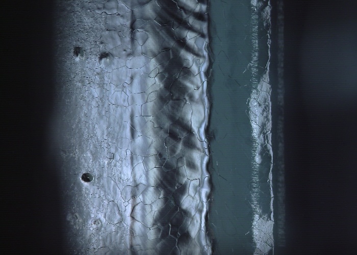 A picture taken with the optical cavity inspection tool. Defects are clearly visible. A picture taken with the optical cavity inspection tool. Defects are clearly visible. |
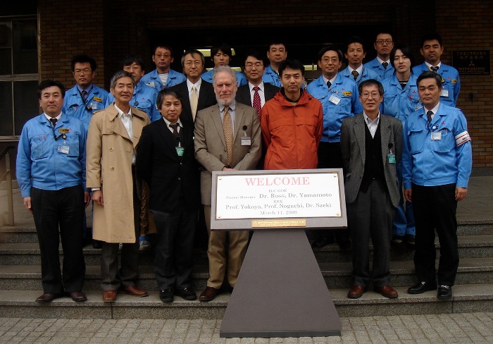 The PM team at the Japanese company MHI on 11 March in Kobe, Japan. The PM team at the Japanese company MHI on 11 March in Kobe, Japan. |
The most important method for cavity diagnostics developed through the GDE gradient study programme is the specialised microscope 'optical inspection' tool that allows precise viewing of structural defects that occur during the fabrication process. Use of this tool in 2008 quickly showed that most of the cavities with a severely limited performance of less than 20 Megavolts per metre exhibited defects in or near the electron-beam weld (EBW) seam used to join the niobium sheet metal sections together. To quote from experts' documentation published during the 1990s: “EBW is a violent process leaving a highly disturbed weld puddle with occasional voids, defects and an irregular surface texture. A surface irregularity can result in local magnetic field enhancement.” Their studies resulted in the widespread adoption of an unusually wide, hot weld bead. A secondary, but more technical, purpose of our visit was to show our recently gathered microscopic photos of the completed welds and try to explain our interpretation of some of the observed features.
Overall, we believe our visits to cavity fabrication companies were a success. We visited Advanced Energy Systems (US), Niowave / Roark (US), Accel (Germany), Zanon (Italy), and Mitsubishi Heavy Industries (Japan) in succession. We are grateful to our hosts for their generous hospitality and would like to extend our deep thanks to them and to the institutional managers who helped organise the visits. In order to establish a standard documentation package to be distributed to each company, we assembled this webpage.
-- Marc Ross